


The data generated by the Internet traffic index growth rate is extremely large, and data centers are critical to supporting the results of data communication, storage, and processing through cloud computing. Optoelectronic devices play a vital role in these data centers, which poses significant challenges for Photovoltaic High Volume Manufacturing (HVM).
Recent Cisco research indicates that global IP and global data center traffic are growing at a compound annual growth rate of approximately 25%. The proliferation of emerging applications such as the Internet of Things (IoT), video streaming, 3D sensing, smart cars and virtual reality (VR) and augmented reality (AR) has created more demand for bandwidth and therefore for new data centers. Demand is growing. Forecasts show that by 2020, 50% of data centers will have a very large scale, which means that the size of its architecture will be able to expand correspondingly with the growth demand added to the system. About 40 hyperscale data centers will be established each year for the next three years.
Optoelectronics is essential for bandwidth growth driven by telecommunications and now driven by digital communications, and electronic communications are driven by the rapid growth of data center services. Figure 1 shows the respective global sales revenue of optical transceivers for telecommunications and data communications. The key turning point is probably 2017–2019, where transceiver revenues for data communications exceed telecom transceiver revenue. The study also predicted a significantly higher growth rate for data communications in the future.
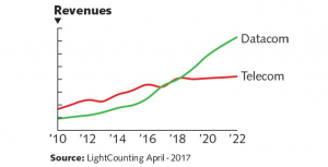
Figure 1. The global sales revenue of optical transceivers for data communications driven by data centers exceeds the global sales revenue of telecom optical transceivers.
Data communication challenge
As data center demand becomes a new growth engine, the optoelectronics industry is experiencing the challenges of serving new data center business model services, which is quite different from traditional telecom models. The chart summarizes the key differences between telecom business models and data center business models. The most critical factors affecting optoelectronic manufacturing are high volume, low predictive visibility, rapid innovation, fast response and low cost.
The influence of telecommunications on the optoelectronic industry has been very large. The reason for telecommunications is that it has a wide field deployment. Due to the difficult working environment (for example: -40 ° C to 85 ° C, relative humidity up to 85%),
Therefore, system deployment and maintenance require high costs, and each telecom upgrade period is long and requires careful planning. The annual forecast from the operator to the equipment supplier to the component supplier is quite good. Precision and expensive optoelectronic components can be accepted for a long time. Optoelectronics manufacturers have a longer time to plan and respond to customer demand, and unit yields are not as high as we have seen in the data center business.
Data center services operate most networks in a controlled environment, such as in buildings where temperature and humidity are controllable (ie, temperature 0–55 ° C, relative humidity 40–60%). Most capital expenditures (capex) are used for land, buildings and wiring. Most operating expenses (opex) are used for energy consumption and environmental control. Optoelectronic components account for a relatively small proportion of capex and opex, but they play a significant role in generating revenue for cloud customers.
In a controlled environment like an office, upgrades become cheaper. Optoelectronic component replacement costs are low and account for a small percentage of the total cost of capex and opex, and the combination of the two enables data center vendors to upgrade their existing data centers every three to five years. For each upgrade, the supplier wanted to maximize the revenue within the same building using the most advanced optoelectronic technology available at the time.
Because the new data center construction project begins with land measurement and acquisition (including approval by local governments), it is difficult for data center suppliers to accurately predict data when data center projects are launched. This greatly reduces the predictive visibility of optoelectronic component suppliers. On the other hand, once the project is approved, data center providers will naturally want to build quickly and rapidly increase revenue streams. Typically after two to three years of construction, the new data center will be ready to run the most advanced optoelectronic devices that will create the greatest revenue potential on the first day.
Finally, for data center applications, rapid innovation presents a dual challenge for high volume and high hybrid optoelectronics manufacturing. The upgrade of transceivers from 10G to 40G is the main activity of the past few years (see Figure 2). Now, 100G is gradually replacing 40G because of the leading technology in new batch deployments. At the same time, the 200/400G solution is in the process of prototyping and small batch production. All of these different technologies and products will need to coexist for a period of time and will all come from the same optoelectronic manufacturing facility.

Figure 2. Shows the coexistence of high-volume, high-mix optoelectronic manufacturing and multi-generation products driven by rapid innovation.
Opportunities and solutions
All of these challenges driven by the new cloud-based data center business model are accompanied by opportunities. How does the photovoltaic industry address these challenges? The key to solving these challenges is automation.
Optoelectronics suppliers do employ an elastic capacity model that enables high-volume, high-quality, low-cost manufacturing and fast switching capabilities in data center timelines, including low predictive visibility (see Figure 3). Automation technology can increase production quickly without worrying about the large amount of training required for high-volume manual production.
Automation technology can also reduce the reliance on labor, thereby reducing variable costs, especially during downtime. In addition, since manufacturers can use the same automation platform and process during development and manufacturing,
Automation technology minimizes the risk of new product introductions (NPIs). In addition, high-precision automation technology enables the production of advanced products using processes that cannot be achieved by hand.
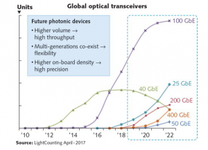
Figure 3. Shows the challenges of the data center business and the possible reactions in the optoelectronics manufacturing arena.
At present, the biggest challenge in the field of optoelectronic manufacturing is how to deal with high-volume and high-mix production. High product mixes often originate from NPIs or from conversions between different products, making this batch production particularly difficult because you can’t increase production while keeping your configuration changing.
Solving this problem requires flexible, high-speed automation technology. Making automation devices both flexible and high speed has always been a challenge. Case studies will show that by innovating in the automation industry, you can achieve high speed while maintaining flexibility.
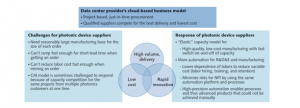
Figure 4. shows an example of various components and automated process combinations in the field of optoelectronic manufacturing.
Flexible high-speed patch automation platform
To clarify our understanding of automation solutions, the following is a case study of one of the key manufacturing processes (ie, patches). Figure 4 is a view of the various components that must typically be fabricated by optoelectronics. Various such parts
Products from different types/generations to support a wide range of data center communication networks. There are several main process steps related to different finished products:
For tube-box products (such as transceivers with high-power lasers), it is common to first complete the substrate/base chip (CoC/CoS) bonding and then bond the CoC/CoS to the lens and mirror attachments. On the substrate, then package. The latest trend is the increasing number of chips or wafers (such as lasers, capacitors, and thermistors) that need to be bonded to a common substrate by eutectic or epoxy bonding.
For PCB layer products such as Active Optical Cable (AOC) and On-Board Optics (OBO), the wafer is attached directly to the PCB. A variety of wafers, such as vertical cavity surface emitting laser (VCSEL) arrays, photodiode (PD) arrays, laser drivers, and transimpedance amplifiers (TIAs), need to be attached to the PCB. The final lens attachment has historically been done by active calibration, but now this process is increasingly being done by passive wafer bonding by a high speed, high precision (3 μm) placement device.
For TO-can products, the laser chip and other wafers are attached to the TO substrate or column after being flipped at 90°. To support the upcoming 5G wireless deployment, wavelength division multiplexing (WDM) lasers and electro-absorption modulated lasers (EMLs) will be packaged in low-cost TO-can packages. These WDM/EML-TOs are much more complex than TO-can packages that only need to handle 1–2 wafers in the case where there are many wafers that need to be bonded.
For silicon photons, there are more and more processes from CoC formation to interposer chip and chip chip (CoW) transition. There are still many processes that have not yet been determined, but the future will increasingly depend on wafer layer integration.
Figure 5 is an example of how to organize automated placement tools and processes for optimal efficiency. There are three columns in this chart: The left side lists examples of integrated placement machines for R&D and small to medium volume production, with the flow coexisting with the process in Figure 4, and the right side for HVM. An example of a flexible high-speed dedicated placement machine.
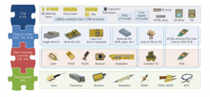
Figure 5. shows an example of a platform approach for high volume, high hybrid optoelectronics manufacturing.
Here are three key points to understand how this approach can help address the optoelectronic manufacturing challenges discussed earlier:
1. A common platform at the hardware and software layers can significantly reduce NPI risk by eliminating control or process changes that have been set up during the development phase. In the R&D/NPI phase, integrated patch devices can be used to develop multiple types of products. Automated machines can handle a variety of wafers and processes in a single device. It is also fast enough to achieve small to medium scale production for design qualifications and manufacturing processes. Once the demand is generated, mass production is required and the production line can be integrated into a specific process group.
- High-volume, high-mix opto-electronic manufacturing requires flexible, high-capacity machines that can cover multiple wafers, processes, and products through one machine for one or more process groups. Optimize speed and throughput by introducing an overspeed eutectic module and deploying multi-stage parallel processing (such as separating material handling from the placement step and zero-time integrated tool change during operation).
- HVM equipment needs to be built for next-generation products for rapid innovation in parallel. For example, 3 μm patch accuracy is improved from current mainstream optoelectronic processes using patch accuracy greater than 5 μm. In addition to implementing new products, the high precision of the patch can increase the process benefits of current product manufacturing by reducing assembly errors as early as possible in the process.
In short, it can achieve 24/7 continuous production, and maintain the original flexibility, accuracy or reliability of high-speed self
The dynamic platform is the key to achieving high-volume, high-mix optoelectronic manufacturing. A common platform between R&D and HVM, as well as timeless accuracy, is also critical to quickly innovating and reducing NPI risk, and increasing production at lower cost in HVM.
